
ABX3lab · Shared resources
Equipment and
techniques.
To take perovskites from material to device, the Associated Unit pools the infrastructure of the ITQ and ICMUV groups: synthesis and processing under controlled atmosphere, optical, electrical and structural characterisation, and indoor and outdoor stability testing.
19
Resources
06
Synthesis & processing
13
Characterisation
01 · Inventory
All the equipment, at a glance.
Search for an instrument or technique, filter by family, switch between list and grid, and open any resource to see its full sheet. Every sheet has its own shareable link.
00
Gloveboxes
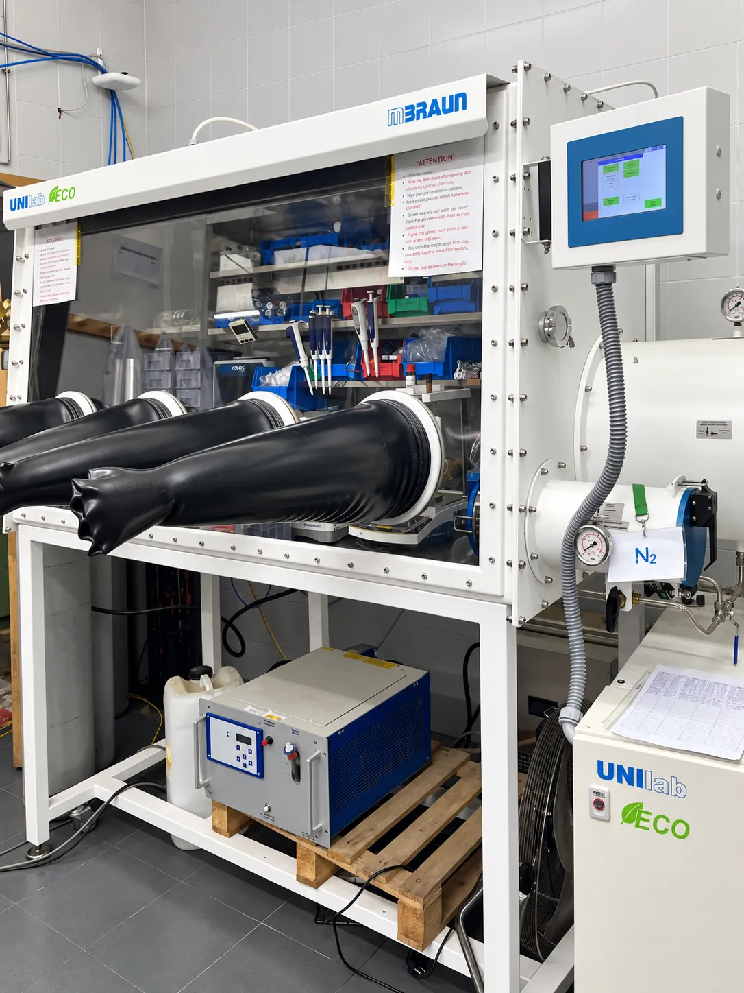
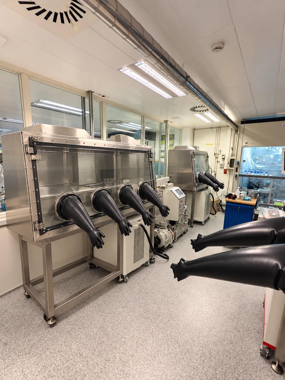
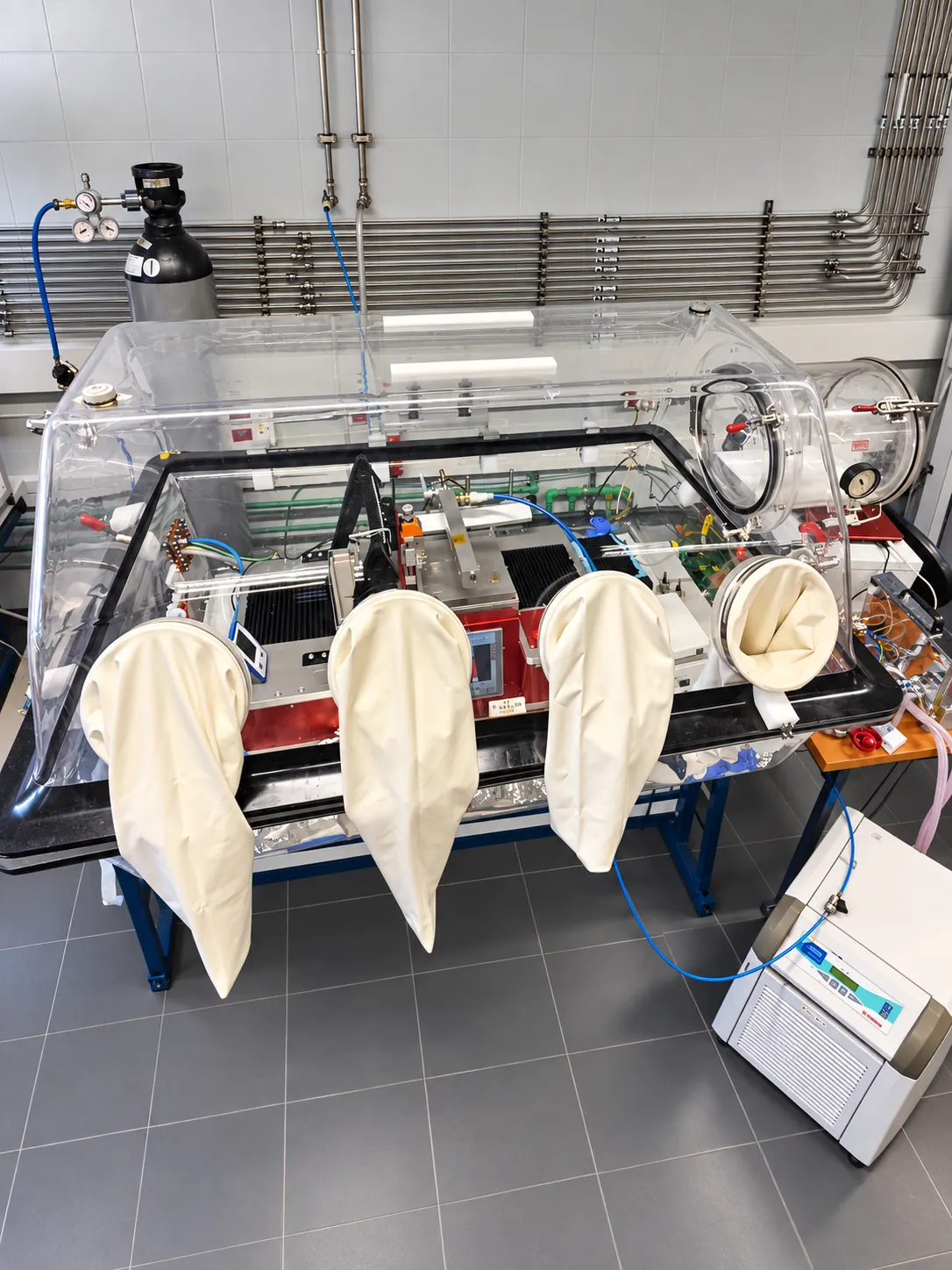
Inert atmosphere Synthesis & processingGloveboxes make it possible to prepare and handle oxygen- and moisture-sensitive materials under a controlled atmosphere. They are essential infrastructure for fabricating thin films and devices based on metal-halide perovskites.
The ITQ laboratories work with argon gloveboxes, while those at ICMUV have nitrogen gloveboxes. These environments allow different preparation and processing steps to be integrated, reducing the samples’ exposure to ambient air.
- Technique
- Handling and processing under controlled atmosphere
- Location
- ITQ — argon · ICMUV — nitrogen
- Inert atmosphere
- Processing
- Sensitive materials
00
Spin coating
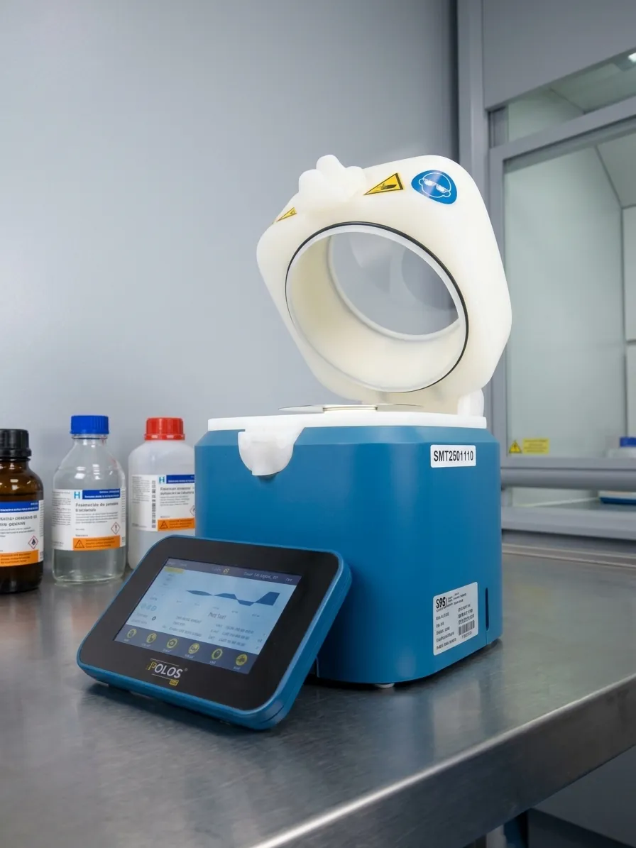
Solution deposition Synthesis & processingSpin coating produces thin films from solutions through the controlled rotation of the substrate. It is used to prepare perovskite layers and other functional materials that form part of optoelectronic devices.
Varying the spin conditions and the formulation makes it possible to study their effect on film formation and device behaviour. Processing inside a glovebox makes it easier to work with air-sensitive compositions.
- Technique
- Film deposition by spin casting
- Location
- ITQ · ICMUV
- Thin films
- Solutions
- Devices
00
Robotic arm
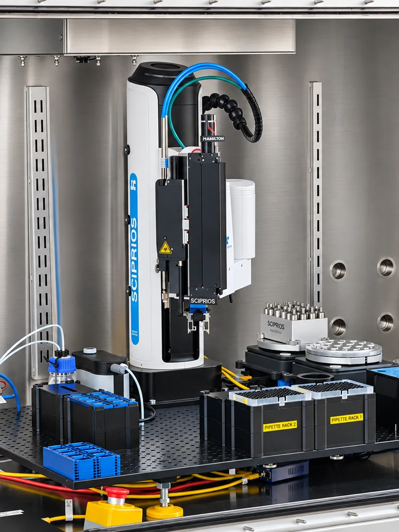
Automated thin-film deposition Synthesis & processingThe robotic arm automates the preparation of thin films from solution. A precision pipetting channel prepares and mixes the inks, a gripper handles vials and substrates, and the layers are deposited by spin coating and then annealed following a programmed recipe.
Because every step is repeated in exactly the same way, it reduces sample-to-sample variability and allows ink composition, spin speed or annealing temperature to be varied systematically. This supports the screening of perovskite compositions and process optimisation with large, reproducible series.
- Technique
- Automated solution processing: pipetting, mixing, spin coating and annealing
- Location
- ICMUV
- Automation
- Reproducibility
- Composition screening
00
Slot-die coating
Scalable deposition Synthesis & processingSlot-die coating deposits thin films from a precursor ink fed to a head with a narrow opening. The controlled outflow of ink and the movement of the substrate relative to the head form a continuous coating, whose solvent is then removed by drying and/or thermal treatment.
It is a scalable technique, particularly suited to developing uniform coatings and large-area devices. Controlling the flow rate, the coating speed and the drying conditions makes it possible to study how the layers form and to carry material optimisation over to larger-area fabrication processes.
- Technique
- Coating through a slot-die head
- Location
- ICMUV
- Upscaling
- Coatings
- Thin films
00
FIRA
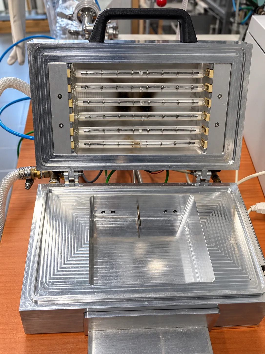
Flash infrared annealing Synthesis & processingFIRA (flash infrared annealing) is a rapid thermal treatment that uses pulses of infrared radiation to heat materials over times ranging from milliseconds to a few seconds, depending on the processing conditions. It can modify the structural, electrical and optical properties of semiconductors and functional layers without prolonged heating.
The group applies it to the study of the drying, formation and transformation of perovskite materials. It is also used to investigate the processing of recovered materials within the circularity research lines, and to compare their response with that obtained through conventional thermal treatments.
- Technique
- Rapid thermal processing with infrared radiation
- Location
- ICMUV
- Rapid processing
- Crystallisation
- Material recovery
00
Thermal evaporation
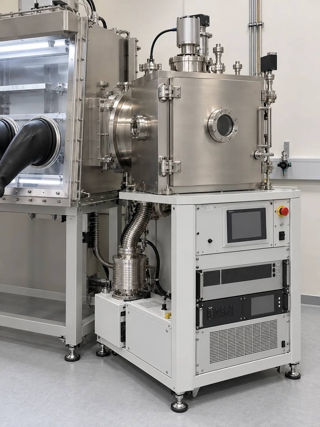
Vacuum deposition Synthesis & processingThermal evaporation deposits thin layers by evaporating a material and condensing it onto the substrate under vacuum. It is used to prepare electrodes and functional layers in optoelectronic devices.
Integration with gloveboxes makes it easier to transfer and process air-sensitive samples. The ITQ incorporates a Korea Kiyon KK-TE/GB-150-2M2O system designed for integration with the Jacomex PUREEVO glovebox.
- Technique
- Physical vapour deposition by thermal evaporation
- Location
- ITQ · ICMUV
- Vacuum
- Functional layers
- Electrodes
00
Photoluminescence
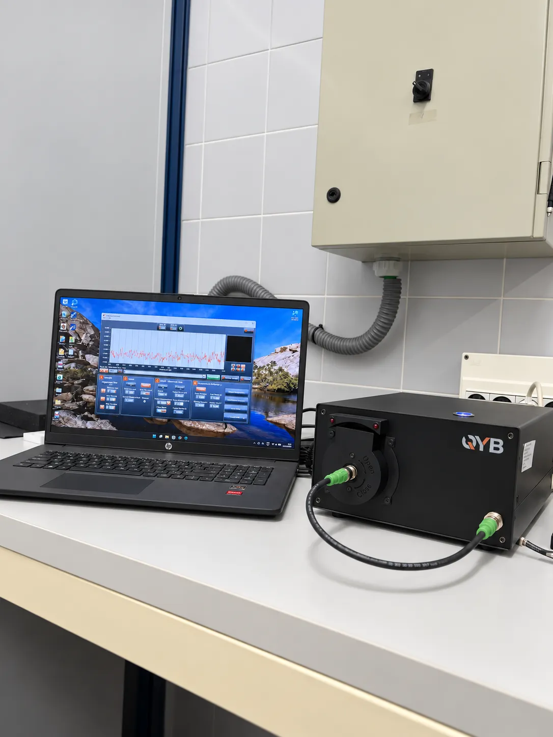
PL, emission dynamics and quantum yield CharacterisationPhotoluminescence studies the light emitted by a material after optical excitation. Emission spectra, their evolution over time and quantum yield measurements provide complementary information on radiative and non-radiative processes.
These measurements make it possible to compare compositions, treatments and processing conditions, and to follow changes associated with perovskite degradation or recovery. They are applied to the photophysical study of materials and to the optimisation of their properties for devices.
- Technique
- Steady-state and time-resolved photoluminescence, and PLQY
- Location
- ITQ · ICMUV
- Emission
- Recombination
- Quantum yield
00
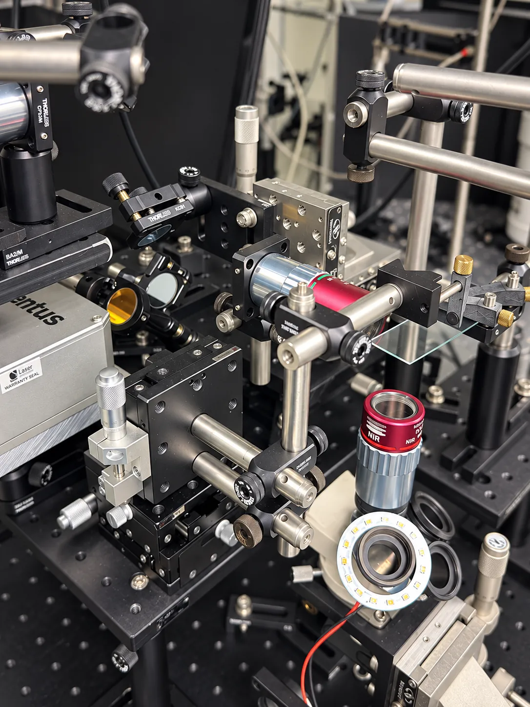
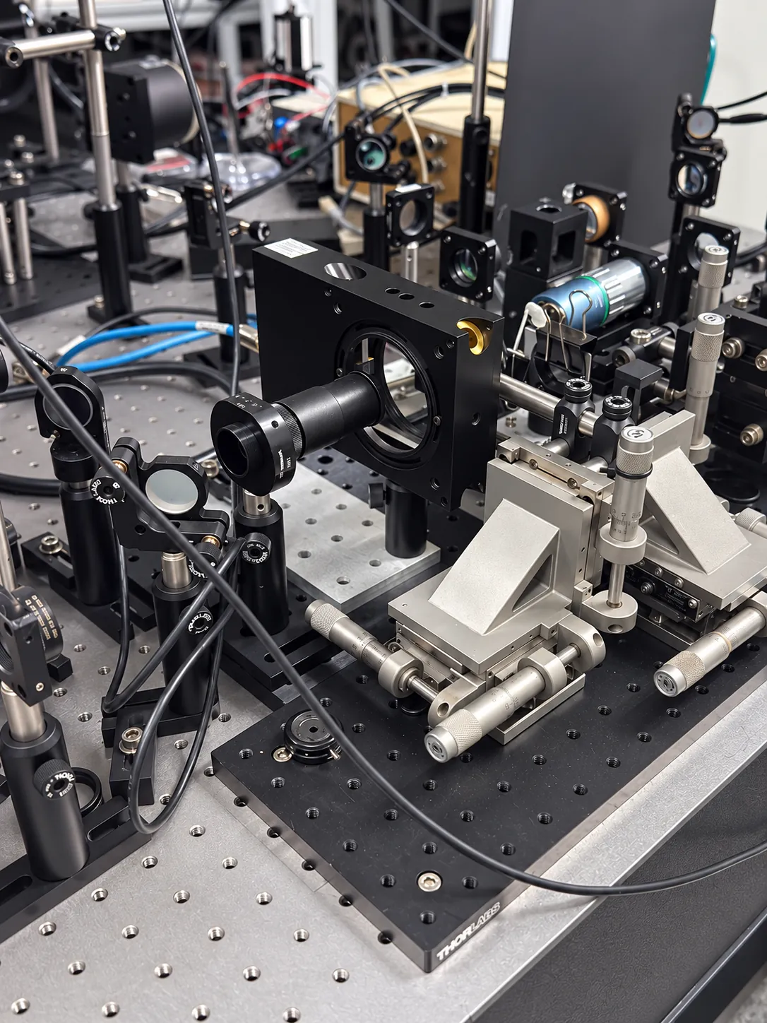
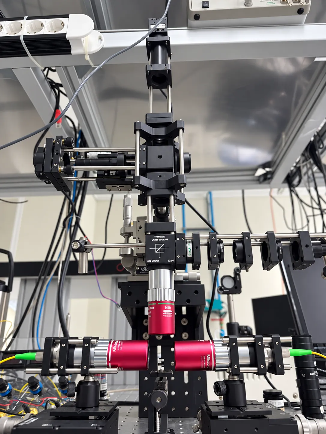
Optical characterisation setups
Photonics, fluorescence and polarisation CharacterisationThe ITQ optical setups make it possible to study the interaction of light with materials and devices through configurations tailored to each experiment. Available capabilities include optical characterisation in fluidic systems, fluorescence, integrated photonics characterisation and circular dichroism.
These experiments provide information on emission, light propagation and polarisation response. A confocal microscopy configuration is also in development to extend the possibilities for spatially resolved characterisation.
- Fluidic optical characterisation
- Fluorescence
- Integrated photonics characterisation
- Circular dichroism
- Confocal microscopy In development
- Technique
- Optical characterisation in experimental setups
- Location
- ITQ
- Integrated photonics
- Fluorescence
- Circular dichroism
00
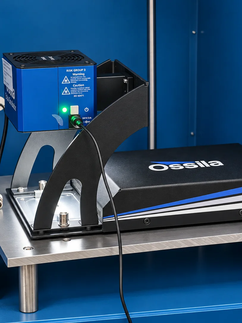
Solar simulator
J–V curves CharacterisationCharacterisation under controlled illumination measures the current–voltage response of solar cells and determines parameters such as the short-circuit current, the open-circuit voltage, the fill factor and the power conversion efficiency.
These measurements make it possible to compare architectures and fabrication conditions, assess reproducibility and study how performance evolves during stability and device recovery tests. Both centres of the Unit, ITQ and ICMUV, have a solar simulator.
- Technique
- Photovoltaic characterisation under controlled illumination
- Location
- ITQ · ICMUV
- Photovoltaics
- J–V curves
- Performance
00
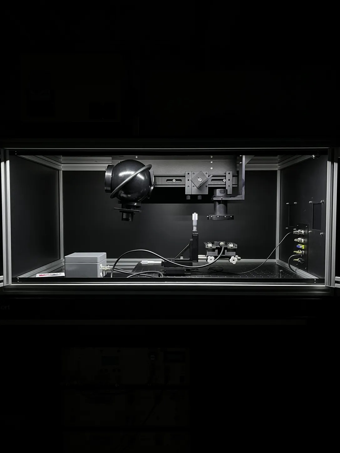
External quantum efficiency · EQE
Photovoltaic spectral response CharacterisationExternal quantum efficiency (EQE) measurement determines the ratio between the electrons collected in the external circuit and the photons incident on a solar cell, as a function of wavelength. It shows which regions of the spectrum contribute to photocurrent generation and allows the response of different materials and architectures to be compared.
The ICMUV setup complements the current–voltage measurements made with the solar simulator. Analysing the spectra helps to assess changes in light harvesting and charge collection; integrating them with a reference irradiance spectrum gives an estimate of the expected short-circuit current density under those conditions.
- Technique
- External quantum efficiency as a function of wavelength
- Location
- ICMUV
- Spectral response
- Photocurrent
- Photovoltaic conversion
00
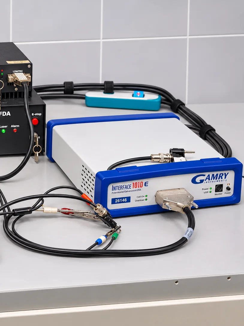
Impedance spectroscopy
Frequency-domain electrical response CharacterisationImpedance spectroscopy analyses the electrical response of a device to a small-amplitude alternating perturbation at different frequencies. It makes it possible to investigate processes on different timescales and complements current–voltage measurements.
In perovskite devices, its interpretation with suitable models helps to study charge transport and accumulation, recombination and the response of interfaces, as well as how they evolve during operation and ageing.
- Technique
- Impedance spectroscopy
- Location
- ICMUV
- Charge transport
- Interfaces
- Electrical dynamics
00
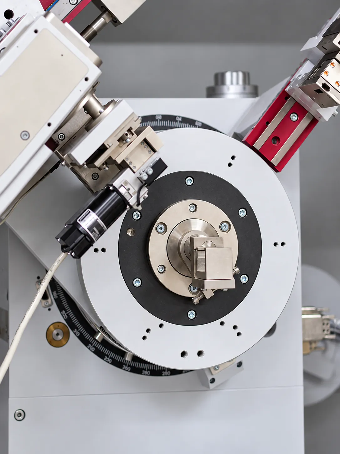
X-ray diffraction · XRD
Crystal structure and phases CharacterisationX-ray diffraction identifies crystalline phases and analyses the structure of materials in powder or thin-film form, depending on the measurement configuration. The resulting patterns allow structural changes associated with composition and processing to be compared.
In the group’s projects, this technique contributes to the study of perovskite formation, degradation and recovery, as well as to the characterisation of recovered materials for reuse.
- Technique
- X-ray diffraction
- Location
- ITQ · ICMUV
- Crystal structure
- Phase identification
- Crystallinity
00
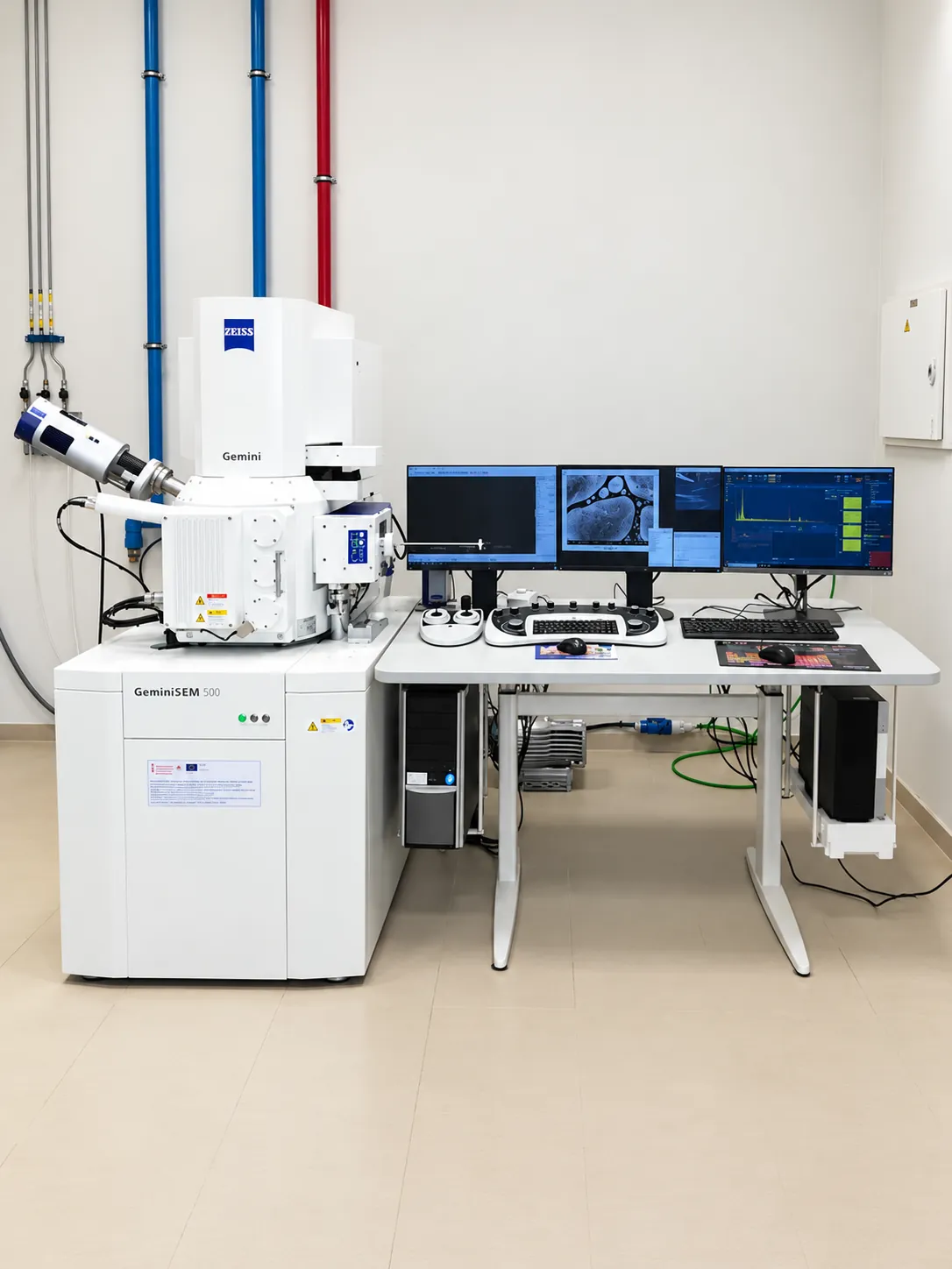
Scanning electron microscopy · SEM
Morphology and microstructure CharacterisationScanning electron microscopy reveals the morphology of surfaces and cross-sections in great detail. It is used to study film coverage, microstructure and the presence of visible discontinuities or defects.
In perovskite materials and devices, it provides information to relate fabrication conditions to the arrangement of the layers and to detect morphological changes after treatments or ageing tests.
- Technique
- Scanning electron microscopy
- Location
- ITQ · ICMUV
- Morphology
- Surfaces
- Cross-sections
00
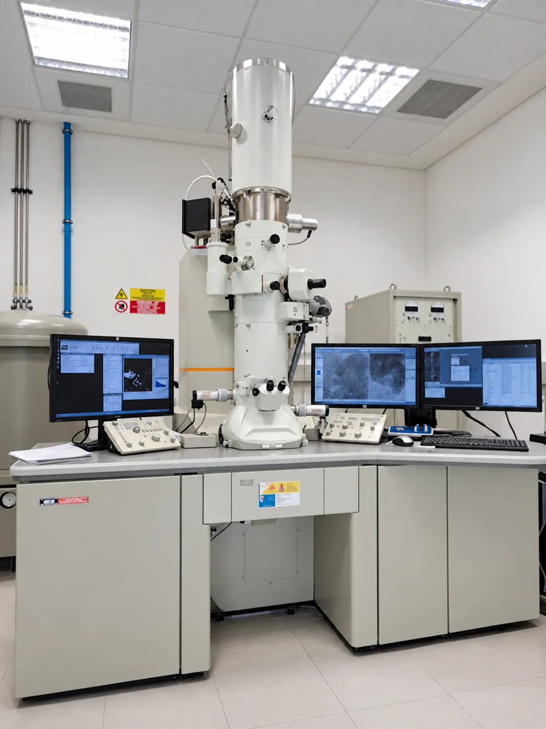
Transmission electron microscopy · TEM
Nanoscale characterisation CharacterisationTransmission electron microscopy studies the internal structure of sufficiently thin samples using transmitted electrons. It provides nanoscale information on the morphology and organisation of materials.
It is a complementary tool for characterising nanocrystals and semiconductor materials, relating their structure to the synthesis conditions and their properties. Sample preparation and imaging conditions are adapted to the sensitivity of each sample.
- Technique
- Transmission electron microscopy
- Location
- ITQ · ICMUV
- Nanostructure
- Nanocrystals
- Internal structure
00
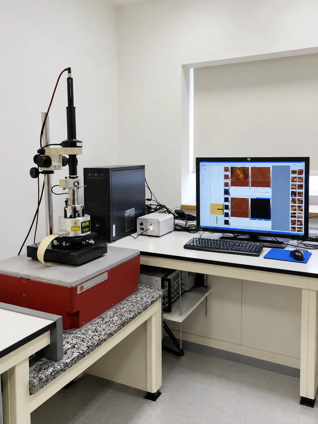
Atomic force microscopy · AFM
Surface topography and roughness CharacterisationAtomic force microscopy produces maps of surface topography through the interaction of a tip with the sample. It is used to analyse texture, roughness and height variations in thin films and other materials.
This information helps to assess coating quality and to study how formulation and processing modify the surface. It complements electron microscopy images and the optical and electrical characterisation of devices.
- Technique
- Atomic force microscopy
- Location
- ITQ · ICMUV
- Topography
- Roughness
- Thin films
00
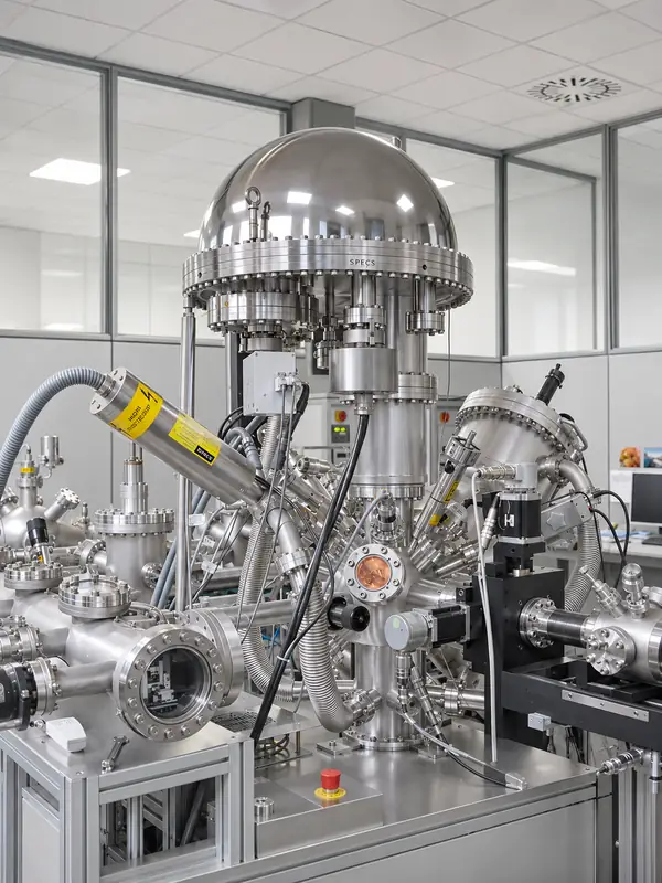
X-ray photoelectron spectroscopy · XPS
Surface composition and chemistry CharacterisationX-ray photoelectron spectroscopy investigates the elemental composition and chemical states of the surface region of a material. It is based on analysing the energy of the electrons emitted after excitation with X-rays.
In the study of perovskites and functional layers, it helps to assess surface modifications, treatments and oxidation or degradation processes. Combined with structural and optical techniques, it makes it possible to relate chemical changes to the behaviour of the material.
- Technique
- X-ray photoelectron spectroscopy
- Location
- ITQ · ICMUV
- Surfaces
- Composition
- Chemical states
00
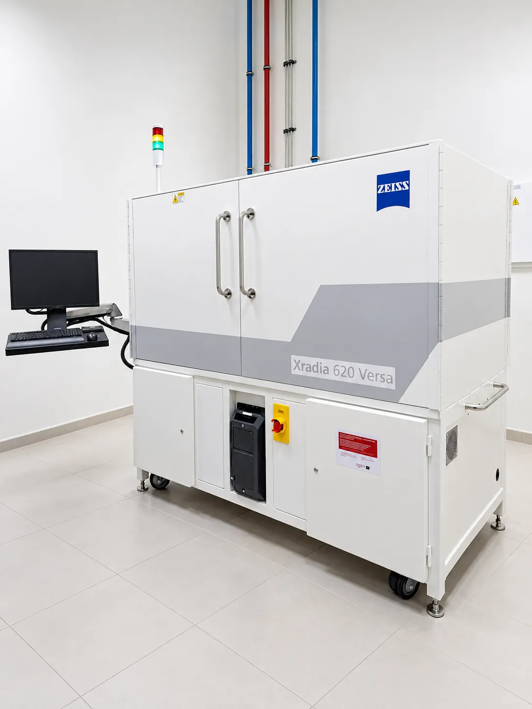
X-ray microscopy · XRM
Internal structure in three dimensions CharacterisationX-ray microscopy explores the internal structure of samples and produces three-dimensional reconstructions through tomographic measurements. Its feasibility and the level of detail that can be observed depend on the size, composition and contrast of the sample.
This technique complements surface characterisation by allowing heterogeneities, porosity or internal defects to be studied in suitable samples. It can support the analysis of structures and components without physically sectioning the sample for each observation plane.
- Technique
- X-ray microscopy and tomography
- Location
- ITQ · ICMUV
- 3D imaging
- Internal structure
- Tomography
00
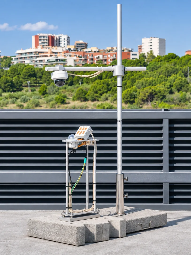
Outdoor testing station
Stability under real conditions CharacterisationOutdoor testing evaluates the behaviour of photovoltaic devices under real solar radiation and ambient conditions. It complements laboratory characterisation and makes it possible to study how performance changes during exposure.
This capability connects the development of materials and encapsulation strategies with the assessment of their stability under real-use conditions. Comparing it with controlled tests helps to understand the differences between ageing in the laboratory and outdoors.
- Technique
- Outdoor photovoltaic testing
- Location
- ITQ · ICMUV
- Stability
- Real operation
- Outdoor exposure
00
PhoenixPV · High throughput
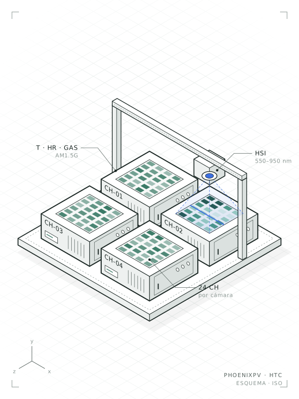
ERC Parallel characterisation CharacterisationThe ERC PhoenixPV high-throughput characterisation platform is designed to follow the evolution of more than a hundred solar cells in parallel. It combines hyperspectral imaging and impedance measurements with four chambers that control light and gas conditions.
Acquiring optical and electrical information together makes it possible to compare series of devices and to study degradation and recovery processes. This infrastructure supports the systematic analysis of materials, interfaces and stabilisation strategies.
- Technique
- High-throughput optical and electrical characterisation
- Location
- ITQ
- Parallel measurements
- Hyperspectral imaging
- Impedance
“ITQ · ICMUV” means availability through both centres, including the shared scientific services of their institutions; it does not imply that the same instrument is installed in both laboratories. To use any instrument, check availability and access conditions.
02 · ERC infrastructure · PhoenixPV
More than a hundred cells, measured at once.
The high-throughput characterisation system of the ERC project PhoenixPV follows more than a hundred solar cells in parallel, with hyperspectral cameras, simultaneous impedance measurements and four chambers where light and gas conditions are controlled.
- 100+ Cells in parallel
- 04 Climate chambers · light & gas
- HSI Hyperspectral imaging
- EIS Simultaneous impedance

- PlatformFour independent climate chambers run in parallel, each with its own temperature, humidity, gas and light.
- Climate chamberInside each chamber, a 60 × 60 mm sample holder connects up to 24 cells to their measurement electronics.
- Solar simulatorAn LED solar simulator illuminates the cells with an AM1.5G-equivalent spectrum.
- j-V curves · MPPEach channel records its j-V curves and tracks the maximum power point: 24 channels per chamber, measured in parallel.
- ImpedanceImpedance spectroscopy runs on the cells of one chamber without stopping the rest of the test.
- Hyperspectral imagingUnder blue excitation, a hyperspectral camera built into the simulator maps luminescence from 550 to 950 nm.
- DataEvery measurement is logged together with its environmental conditions and shared on NOMAD.
- c1
- Chamber 0185 °C · 85 % RH
- c2
- Chamber 0225 °C · AM1.5G
- c3
- Chamber 0365 °C · dry N₂
- c4
- Chamber 04−10 °C · dark
- gas
- Gas
- led
- LED solar simulator
- holder
- Sample holder60 × 60 mm
- sensor
- T · RH sensor
- ecb
- Measurement electronics
- beam
- AM1.5Gilluminated area 5 × 5 cm
- eis
- Impedance module
- cable
- Per chamberwithout stopping the test
- cam
- Hyperspectral camera
- cube
- Data cubex · y · λ
- power
- Control and synchronisation
- nomad
- NOMADopen data
- chipT
- T · 10–90 °C
- chipH
- RH · ≥ 70 %
- chipG
- Controlled gas
- chipL
- AM1.5G light
- dim
- 60 mm
- chan
- Channel
- g_jv
- j-V curve · MPP
- g_nyq
- Nyquist
- g_nyq_n
- Frequency response
- g_spec
- PL spectrum
- g_spec_n
- 550–950 nm · ≤ 5 nm
- pause
- Pause
- play
- Play